Professor Yaping Dan’s research team at the University of Michigan- Shanghai Jiao Tong University Joint Institute (UM-SJTU JI) has published a research article in ACS Nano, titled “Dynamics of Charge Carriers in Silicon Nanowire Photoconductors Revealed by Photo Hall Effect Measurements”. The research team employed Photo Hall effect to investigate the charge carrier dynamics in a single silicon nanowire photoconductor. The results revealed the mechanism of extraordinarily high photo gain that is often observed in nanoscale photoconductors. Professor Yaping Dan is the corresponding author of the paper and Mr. Kaixiang Chen, a PhD candidate in Professor Dan’s research team is the first author. Professor Yongning Her from Xi’an Jiao Tong University is the co-corresponding author.
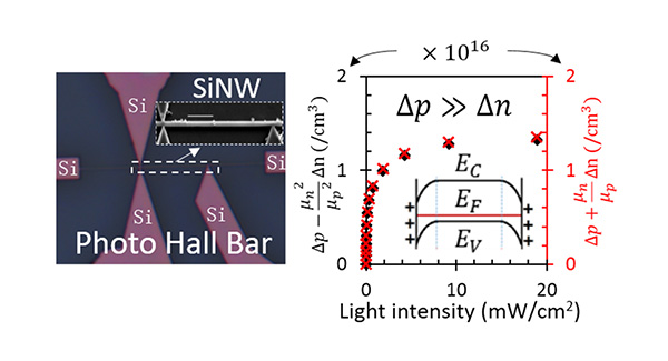
 Optical microscopic image of device structure and experimental data.
In theory, semiconductor photoconductors have no gain or at least no high gain. But it is often reported that nanoscale photoconductors have a gain in quantum efficiency up to 8 orders of magnitude. In the past 60 years, similar high gains are frequently reported on photoconductors based on thin films, nanowires and more recently two-dimensional atomically thin crystals. Researchers proposed many mechanisms to explain the high photo gain. However, photoconductors remain more like a “black box”. The exact mechanism for this high gain is still in dispute.
In this published work, Professor Dan and his team uncovered the nanowire photoconductor “black box” by investigating the dynamics of charge carriers in a silicon nanowire by Photo Hall effect. The results show that photogenerated majority carriers (holes) in the nanowire channel outnumber the excess minority electrons by orders of magnitude, leading to the widely observed high photo gain. But it is well known that the excess electrons and holes are excited in pairs by light illumination. Thus, the number of excess electrons and holes should be equal. The research work further shows that this unexpected inequality of excess electrons and holes in the nanowire channel is caused by nanowire surface states that capture a large number of photogenerated electrons (removed out of the channel and localized on the nanowire surfaces). The same number of excess holes is left in the nanowire conduction channel. Photo Hall effect can only measure the concentration of charge carriers in the channel instead of those trapped in the surface states. This explains the aforementioned inequality of excess electrons and holes in the nanowire channel.
This research finding reveals the gain mechanism of nanoscale photoconductors and will guide researchers to design high speed and high gain photodetectors. The work is financially supported by National Science Foundation of China (NSFC 61376001) and the Major Research Plan, Science and Technology Commission of Shanghai Municipality (16JC1400405).
Background Information
Dr. Yaping Dan is an Associate Professor of electrical engineering at the UM-SJTU Joint Institute. He received his bachelor’s degree in electrical engineering from Xi’an Jiaotong University in 1999, master’s degree in microelectronics from Tsinghua University in 2002, and doctoral degree in electrical engineering from the University of Pennsylvania in 2008. Before he joined the Joint Institute, he was a postdoctoral fellow and then research associate at Harvard University. He won the postdoctoral fellowship award from the US National Academies in 2009. He served as the editorial board member of Scientific Reports since 2016 and an adjunct professor at Xi’an Jiaotong University since 2017.
ACS Nano is a top peer-reviewed research journal of the American Chemical Society. The journal publishes original research articles, reviews, perspectives, interviews with distinguished researchers, views on the future of nanoscience and nanotechnology.


